Difference between revisions of "Hardware:Memory Map"
From Motorola 68000 Homebrew Computer Project
| Line 9: | Line 9: | ||
Memory mapped I/O area from 0x00200000 - 0x003FFFFF will be broken down with another 74LS138 into 8 256KB chunks or maybe with a 4-to-16 decoder for 16 chunks. | Memory mapped I/O area from 0x00200000 - 0x003FFFFF will be broken down with another 74LS138 into 8 256KB chunks or maybe with a 4-to-16 decoder for 16 chunks. | ||
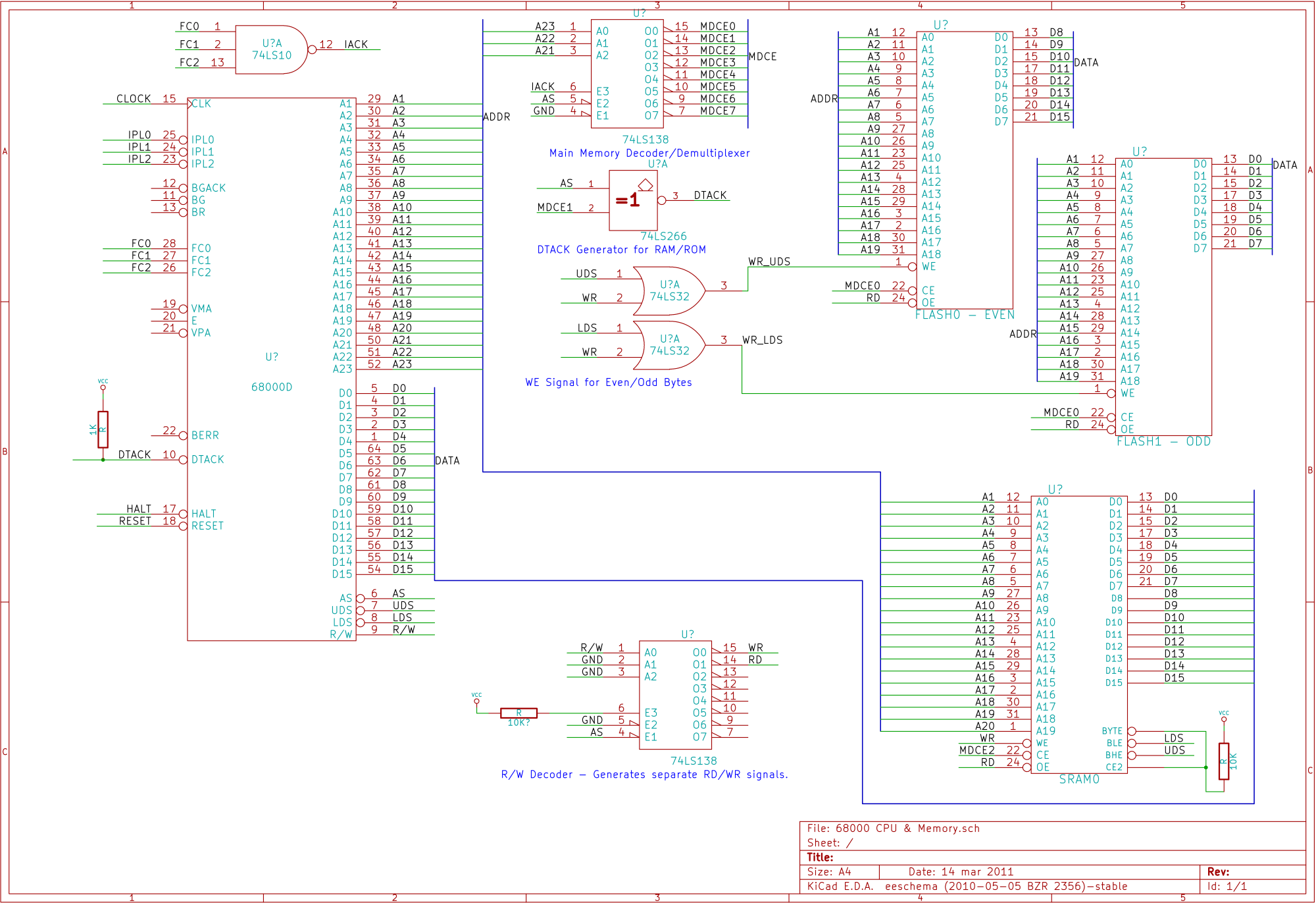
| − | Here is my WIP memory decoder showing flash ICs and one SRAM. | + | Here is my WIP memory decoder showing flash ICs and one SRAM. There will be a total of 6 SRAMS for a total of 12MB RAM. SRAM0-SRAM5 will be wired exactly the same way execpt different MDCE pins (MDCE2-MDCE7). |
[[Image:memdec.png]] | [[Image:memdec.png]] | ||
Revision as of 07:41, 10 March 2011
The 16MB of address space will be broken up into 8 2MB chunks by a 74LS138 3-to-8 decoder.
0MB: 0x00000000 - 0x000FFFFF ROM 1 MB
1MB: 0x00100000 - 0x001FFFFF Reserved 1 MB, possible future use for more memory mapped I/O or VRAM, etc.
2MB: 0x00200000 - 0x003FFFFF Memory Mapped I/O 2 MB
                             Device Map
4MB: 0x00400000 - 0x00FFFFFF Static RAM 12 MB
Memory mapped I/O area from 0x00200000 - 0x003FFFFF will be broken down with another 74LS138 into 8 256KB chunks or maybe with a 4-to-16 decoder for 16 chunks.
Here is my WIP memory decoder showing flash ICs and one SRAM. There will be a total of 6 SRAMS for a total of 12MB RAM. SRAM0-SRAM5 will be wired exactly the same way execpt different MDCE pins (MDCE2-MDCE7).

