Difference between revisions of "Schematic:CPU, Memory, and Main Memory Decoder"
From Motorola 68000 Homebrew Computer Project
| (3 intermediate revisions by the same user not shown) | |||
| Line 1: | Line 1: | ||
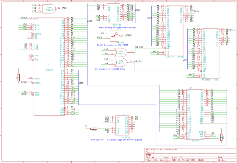
Here is my WIP memory decoder showing flash ICs and one SRAM. There will be a total of 6 SRAMS for a total of 12MB RAM. SRAM0-SRAM5 will be wired exactly the same way execpt different MDCE pins (MDCE2-MDCE7). | Here is my WIP memory decoder showing flash ICs and one SRAM. There will be a total of 6 SRAMS for a total of 12MB RAM. SRAM0-SRAM5 will be wired exactly the same way execpt different MDCE pins (MDCE2-MDCE7). | ||
| − | |||
| − | |||
<imagemap> | <imagemap> | ||
Image:memdec.png|800px|alt=CPU, Memory, and Main Memory Decoder Circuit|Image map example. Clicking on a person in the picture causes the browser to load the appropriate article. | Image:memdec.png|800px|alt=CPU, Memory, and Main Memory Decoder Circuit|Image map example. Clicking on a person in the picture causes the browser to load the appropriate article. | ||
| − | rect | + | rect 284 149 540 972 [[Hardware:CPU|68000 CPU]] |
| + | rect 1393 48 1537 469 [[Hardware:ROM|512Kx8 FLASH]] | ||
| + | rect 1695 240 1840 661 [[Hardware:ROM|512Kx8 FLASH]] | ||
| + | rect 1565 752 1713 1171 [[Hardware:RAM|1Mx16 Static RAM]] | ||
</imagemap> | </imagemap> | ||
Latest revision as of 15:32, 12 March 2011
Here is my WIP memory decoder showing flash ICs and one SRAM. There will be a total of 6 SRAMS for a total of 12MB RAM. SRAM0-SRAM5 will be wired exactly the same way execpt different MDCE pins (MDCE2-MDCE7).